


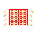
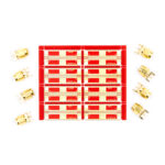

Experimental Set of 8 pcbs with 50 Ohm CPW not soldered SMA connectors VNA teach (DIY KIT)
37,07 €
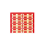
RF Experimenter’s VNA-test PCB Panel of 8 pcs (DIY KIT)
Only 2 left in stock
This product is a complete KIT consisting of a panel of 8 PCBs, hand-breakable for easy separation, implementing a 50 Ω Co-Planar Waveguide over Ground (CPW-G) transmission line.
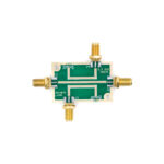
The design provides dedicated areas for Short / Open / Load terminations as well as a DUT (Device Under Test), enabling RF performance and signal integrity measurements.
The experimenter can place and evaluate a wide variety of DUTs. These may range from a simple decoupling capacitor used in digital power rails—allowing characterization of capacitance versus applied DC voltage, frequency, or pulse excitation—to more complex passive or active circuits with 50 Ω input and output ports.
Multiple capacitors connected in parallel, a common practice in RF and high-speed digital designs for DC rail decoupling, can also be placed and characterized using an appropriate measurement methodology, with or without applied DC bias.
Modern high-speed digital circuit design requires solid RF knowledge and experience. It is a demanding and highly specialized field of technology. This compact and versatile PCB panel serves as a practical tool for students, engineers, and experimenters, supporting hands-on learning and contributing to the improvement of design and implementation skills.
The use of an expensive Vector Network Analyzer (VNA) is not mandatory. While a VNA is undoubtedly a powerful instrument, many meaningful measurements can be performed using alternative equipment such as a multimeter, a phase detector (e.g., an AD8302 module), a directional coupler, a power detector, a DC power supply, an oscilloscope, and a pulse or signal generator. Not owning a VNA often encourages the development of creative and efficient measurement techniques.
The PCB is manufactured on FR4 substrate, therefore it is not intended for applications above approximately 3–4 GHz. For lower-frequency work, however, this panel is well suited to most practical needs. For example, when characterizing power distribution components, measurements are typically performed from 100 Hz up to 10 MHz, or up to 100 MHz, i.e. approximately one decade above the series resonance frequency of the DUT.
Kit Contents
1 high-quality ENIG-finished FR4 PCB panel
Dimensions: 73.5 × 63.5 mm
8 male SMA connectors
8 female SMA connectors
(connectors supplied not soldered)
A version with pre-soldered SMA connectors is also available—please refer to our related products.